

Known PCB Assembly: Essential Techniques for Reliable Circuit Boards
2026-06-10
Every circuit board holds the promise of flawless performance—until a hidden assembly flaw brings it to a halt. Known PCB assembly isn't just about following a checklist; it's about mastering the essential techniques that transform a good design into a truly reliable product. From solder paste secrets to thermal stress management, the difference lies in the details most guides overlook. At TPS, we've seen how small, smart choices in assembly can prevent field failures and elevate board longevity. Ready to uncover the core practices that separate dependable boards from costly reworks? Let's dive into the proven methods that keep your circuits running strong.
Precision Soldering: The Backbone of PCB Reliability
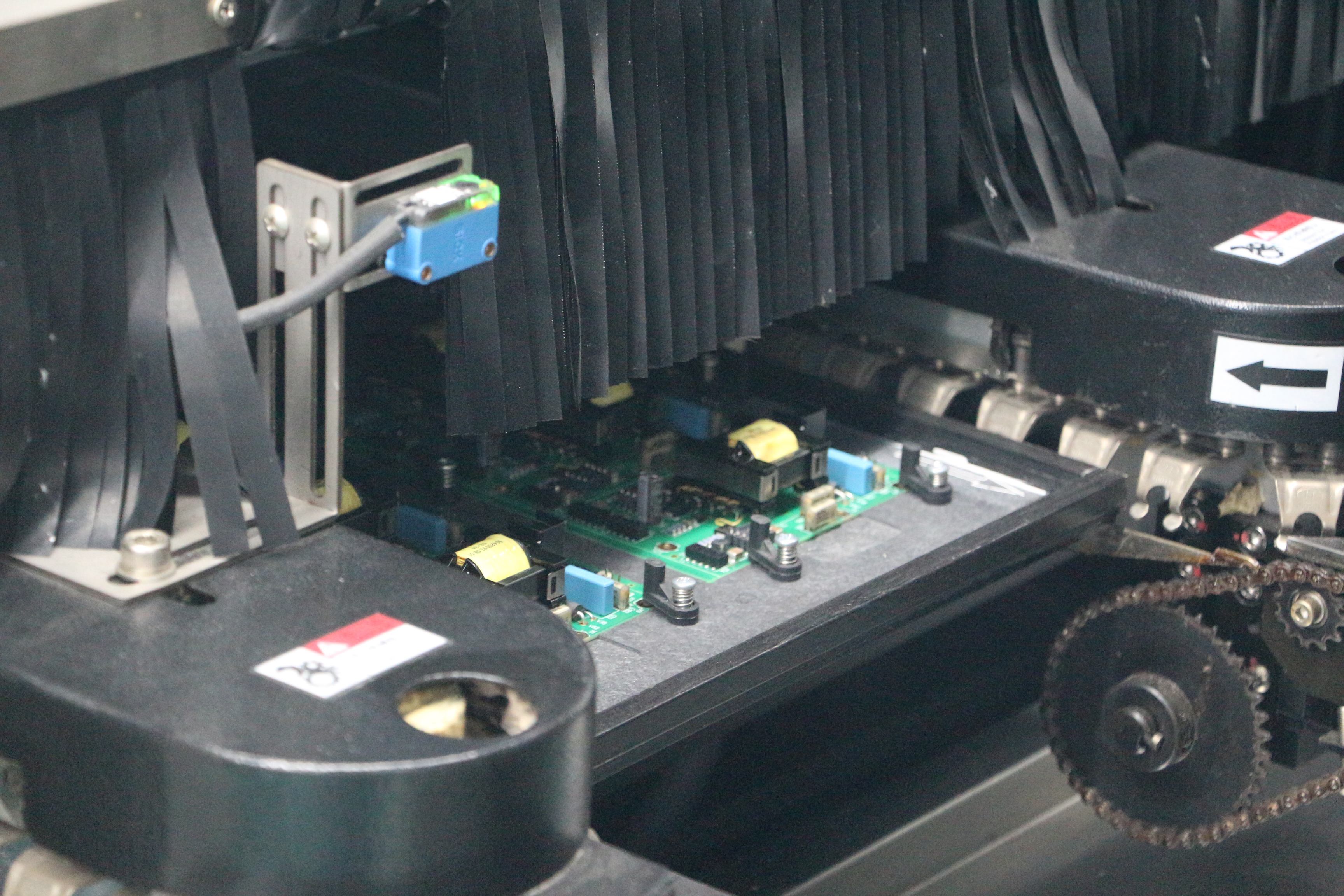
Every electronic device hinges on the silent integrity of its printed circuit board, and at the heart of that integrity lies precision soldering. It’s not merely about joining components to a board—it’s the craft of creating metallurgical bonds that endure thermal cycling, mechanical stress, and years of operation without a whisper of failure. A single cold joint or a micro-fracture invisible to the naked eye can unravel the performance of an entire system, turning a sophisticated design into a costly paperweight. In high-stakes industries, from medical implants to aerospace avionics, the margin for error doesn’t exist; soldering must be flawless, repeatable, and tailored to the specific demands of each assembly.
Achieving such reliability demands a blend of rigorous process control, deep material science, and skilled human judgment. Modern precision soldering navigates tighter pad pitches, heat-sensitive components, and the quirks of lead-free alloys that behave differently across narrow temperature windows. It’s a discipline where oxidation, flux chemistry, and tip geometry are scrutinized as closely as the soldering iron’s calibration. Automated optical inspection can catch many flaws, but it’s the trained technician who interprets the subtle sheen of a perfect joint or the faint grainy texture of a disturbed one. Without this meticulous approach, even the most advanced PCBs remain vulnerable to latent failures, proving that precision soldering isn’t just a step in assembly—it’s the backbone that carries the weight of modern electronics.
Mastering SMT Component Placement for Flawless Boards
Getting SMT component placement right isn’t just about running a pick-and-place machine at high speed. The real magic happens when each part lands on its pads with sub-millimeter accuracy, regardless of its size or shape. Even a tiny shift can create tombstoning, bridging, or cold joints that become headaches during inspection.
Board designers often forget how much the pad layout and stencil design influence placement success. A poorly defined footprint can cause a chip to float out of position during reflow, especially with miniature passives. Paying attention to solder paste volume and land pattern symmetry goes a long way before the first component ever hits the board.
Modern equipment offers vision alignment and real-time correction, but seasoned operators know that a clean, well-maintained nozzle and a deliberate part-feed setup matter just as much. Sometimes slowing down the line slightly to let the vision system do its job eliminates more defects than any high-speed run ever could.
Ensuring Signal Integrity with Controlled Impedance Routing
Getting a clean signal across a high-speed PCB trace isn't just about connecting point A to point B. When rise times shrink below a nanosecond, the trace behaves less like a simple wire and more like a transmission line. Controlled impedance routing means designing that trace with a specific target impedance—often 50 ohms for single-ended or 100 ohms for differential pairs—so that the driver, line, and receiver are all in harmony. Without it, reflections bounce back and forth, eating into your noise margins and corrupting data eyes.
The magic lies in the geometry and materials. Trace width, thickness, and spacing to the reference plane form the backbone, while the dielectric constant of the substrate sets the wave speed. A slight change in any of these—say, an unexpected deviation in core prepreg thickness—can skew impedance enough to cause noticeable ringing. That's why fabricators need tight tolerances and why designers obsess over etch factor and glass weave effects. Even vias, with their stray capacitance, need careful modeling if you're pushing beyond a few GHz.
Practically, it's a balancing act during layout. You might juggle line widths to hit impedance targets while keeping crosstalk in check, or play with differential pair spacing to nail that 100-ohm sweet spot. Simulation tools help, but there's no substitute for a good stack-up and clear fab notes. Some teams even prototype with TDR measurements to catch impedance valleys before they become system-level headaches. When done right, controlled impedance routing turns a frantic debug session into a routine bring-up.
Thermal Management: Preventing Hotspots in High-Density Designs
As component densities climb, so does the risk of localized heat buildup that can throttle performance or cause premature failure. The trick lies in spreading thermal loads intelligently, not just slapping on bigger heatsinks. By placing high-power components along natural airflow paths and staggering them to break up thermal wakes, you can keep junction temperatures from creeping into dangerous territory without resorting to exotic cooling methods.
Board-level decisions make or break hotspot mitigation. Copper pours, via stitching, and thick internal planes act as silent heat spreaders, pulling energy away from tiny hotspots and into the board’s mass. Even a simple tweak like orienting a buck converter’s inductor to minimize magnetic heating in adjacent traces can drop local temperatures by several degrees. It’s these granular, almost invisible choices that compound into a robust thermal design.
Don’t overlook the enclosure’s role in the thermal puzzle. A poorly placed vent or forgotten gasket can starve your carefully crafted layout of airflow, turning a minor warm spot into a full-blown hotspot under sustained load. Prototyping with thermal imaging early, while iterating on vent placement and board-to-chassis conduction paths, reveals problems simulation alone misses. The goal is a design where heat moves so seamlessly that hotspots never get a chance to form.
The Art of Cleanliness: Flux Removal and Contamination Control
Cleanliness in electronics assembly isn't just about wiping down surfaces—it's a discipline that begins the moment flux touches a board. Every type of flux, whether rosin-based, water-soluble, or no-clean, leaves behind residues that can quietly undermine reliability. Rosin fluxes, for instance, form hard, glassy deposits that might look innocent but can trap corrosive activators underneath. Water-soluble variants demand aggressive washing with deionized water, often within a tight window after soldering, or their residues turn conductive and start corroding copper traces. No-clean formulations promise convenience, yet even they can leave behind a thin, often invisible film that interferes with conformal coating adhesion or causes leakage currents in high-impedance circuits. Understanding the chemistry of the flux you're using is the first step toward effective removal.
Choosing the right cleaning method is where the art really comes into play. Manual scrubbing with an ESD-safe brush and a solvent like isopropyl alcohol works for small batches, but it introduces variability—pressure, dwell time, and solvent purity all shift results. Automated inline washers offer consistency, using heated sprays or ultrasonic agitation to flush residues from under low-standoff components. Yet even automation has its quirks: spray bar angles, belt speed, and rinsing stages must be tuned for each board design. Sometimes a hybrid approach is best, like a targeted solvent dispense on a specific connector followed by a full aqueous rinse. Testing for cleanliness afterward is non-negotiable; resistivity of solvent extract (ROSE) tests give a bulk ionic reading, but ion chromatography reveals exactly what's lurking on the surface, helping you connect cleanliness levels to field failures.
Contamination control extends beyond flux, encompassing particles, fibers, and plating salts that sneak in during handling or storage. A fingerprint left on a gold contact can create a microclimate for corrosion, and a stray solder ball lodged under a BGA might cause a latent short that passes initial testing but fails months later. Cleanroom disciplines—like proper gowning, sticky mats at doorways, and regular surface wipe-downs—reduce this background noise. For high-reliability applications, such as aerospace or medical devices, even the packaging materials are scrutinized; outgassing from tape or foam can re-deposit volatiles onto critical surfaces. Building a contamination control plan means mapping every step from bare board to final assembly, identifying where unwanted materials might hitch a ride, and designing them out of the process entirely. The payoff is a product that performs not just on day one, but through years of harsh operation.
Testing Protocols That Catch Failures Before Production
Pre-production testing isn't about checking boxes on a compliance form. It's a deliberate attempt to break the system in controlled ways before a user stumbles into the mess. Teams that get this right treat failures as data points, not personal shortcomings. A battery of edge-case injections, load spikes timed to coincide with cache expiry, and race conditions triggered by unnatural event ordering—these are the real gatekeepers. No amount of unit test coverage can substitute for observing what actually crumbles when you pull the scaffolding away.
The protocol design often matters more than the tests themselves. Multi-stage validation sequences that escalate complexity gradually tend to surface cascading failures that single-pass checks miss. For instance, running a soak test immediately after a data migration, then throwing in a network partition during the final assertion window, can reveal timeout assumptions that looked solid on paper. The trick is chaining stressors so the system never fully recovers between them—mimicking the kind of cumulative degradation that takes down production environments on a Tuesday afternoon.
What separates mature protocols from amateur hour is the post-failure analysis loop. It's not enough to log an exception and schedule a retry. Every caught failure gets reverse-engineered to its weakest signal: the log message that was a millisecond late, the metric that flattened ten seconds before the alert threshold, the config flag that defaulted to a dangerous value only under a specific feature flag combination. These artifacts get woven directly into the next iteration of the protocol, so the same class of failure can't trick the system twice. Over time, the test suite becomes a physical model of your system's fragility—and running it feels less like verification and more like a pre-flight system integrity check that you'd be genuinely uneasy to skip.
FAQ
PCB assembly is the process of soldering electronic components onto a printed circuit board to create a functional device. It's critical because the quality of assembly directly impacts the performance, durability, and reliability of the final product. Poor assembly can lead to failures, short circuits, or complete malfunction.
Surface-mount technology (SMT) involves placing components directly onto the board's surface, allowing for smaller, lighter, and more automated assembly. Through-hole technology (THT) requires inserting component leads into drilled holes and soldering them on the opposite side, offering stronger mechanical bonds for components subject to stress. The choice depends on the design's size constraints and mechanical demands.
Solder paste, a mixture of tiny solder spheres and flux, is applied to the board before component placement. It holds components in place temporarily and, when heated, melts to form permanent electrical and mechanical joints. Using high-quality paste with the right viscosity and composition prevents defects like bridging or insufficient wetting.
A reflow soldering profile defines the temperature curve the board follows through the oven. It's essential because improper heating can cause thermal shock, component damage, or incomplete solder joints. A well-designed profile ensures gradual preheating, proper soak time, and peak temperature, leading to consistent, reliable connections.
Inspection catches defects like misaligned components, solder bridges, or insufficient solder before they cause field failures. Automated optical inspection (AOI) and X-ray inspection are common methods that verify joint quality and hidden connections, especially for ball grid arrays. Skipping inspection risks costly rework or product recalls.
Look for a partner with certified processes (like IPC standards), robust quality control, and experience with your type of board. They should offer design for manufacturability (DFM) feedback, have advanced equipment, and provide traceability. A reliable partner helps avoid production delays and ensures consistent output.
Excessive heat during operation or assembly can degrade components and solder joints. Proper thermal management involves using heat sinks, thermal vias, and choosing materials with appropriate coefficients of thermal expansion. During assembly, controlling reflow profiles and using thermal relief patterns on large copper areas prevents warping and soldering issues.
Common mistakes include inadequate cleaning leaving residues, incorrect component orientation, using expired or poor-quality solder paste, and skipping design rule checks. These can lead to corrosion, intermittent connections, or electrostatic damage. Strict process controls and thorough training mitigate these risks.
Conclusion
Precision soldering is more than just melting alloy—it requires careful temperature profiling to avoid cold joints or component damage, especially with lead-free alloys that demand tighter process windows. Mastering SMT component placement involves not only high-speed pick-and-place equipment but also verification through automated optical inspection to catch tombstoning or skew immediately after placement. Together, these fabrication steps create the physical backbone of a PCB assembly, where every joint and component must survive thermal cycling and mechanical stress over the product's lifetime.
As operating frequencies rise, controlled impedance routing becomes non-negotiable for preserving signal quality, requiring close collaboration between design and fabrication to maintain consistent trace geometry and dielectric properties. Effective thermal management prevents hotspots that accelerate wear, using techniques like thermal vias and heat-dissipating planes to spread heat away from sensitive components. Cleanliness is another often underestimated factor: incomplete flux removal can lead to electrochemical migration, causing intermittent failures that are notoriously hard to diagnose. The final safeguard lies in comprehensive testing—combining flying probe, boundary scan, and functional tests—which simulates real-world conditions to weed out marginal units before they reach the field.
Contact Us
Contact Person: Lily
Email: [email protected]
Tel/WhatsApp: +49 (0) 2161 49526-0
Website: https://tps-elektronik.com/en/